Blog
From Schematic to Board: How PCBs Are Made
A PCB is a wiring diagram made of copper: the schematic drawn in metal so the wiring can be printed a million times. Here is how PCBs are made, from copper-clad fibreglass and light to the reflow oven.
 Tan Kok XinElectricity Fundamentals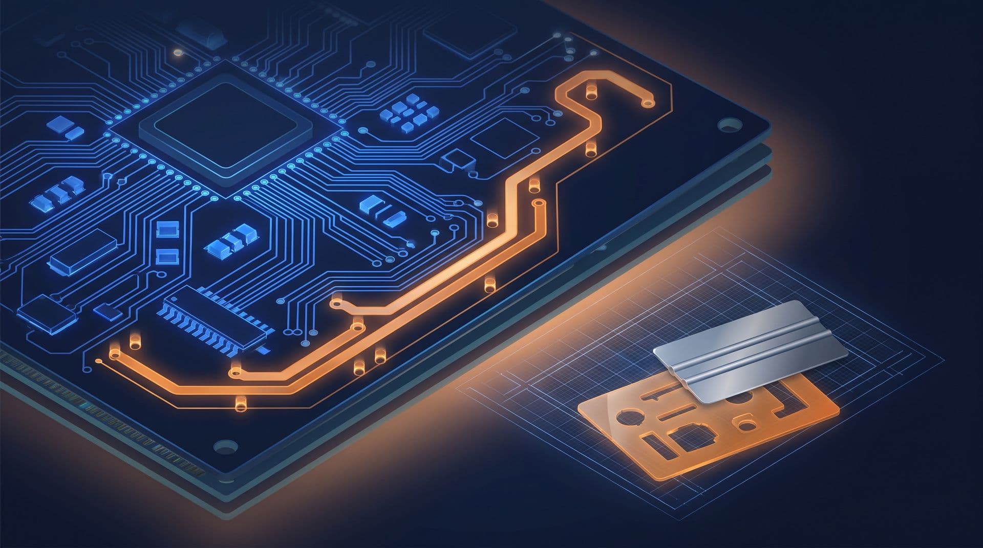
A Silicon Annex extra to Cobler's Electricity Fundamentals course: the course's story, continued from electrons into computation.
Take the cover off almost anything in the switchroom, a kWh meter, a small controller, the driver board inside a VFD, and you meet the same object every time: a flat green board with silver-grey lines threading across it and black components soldered on top. It is the printed circuit board, the substrate inside nearly every electronic device on Earth. And almost nobody who handles one daily can say how PCBs are made. That is worth fixing, because the answer is far simpler than the board looks, and once you have it, every green rectangle in the panel stops being a sealed mystery and turns into something you can read.
You have probably held hundreds of these boards without ever asking the obvious thing: where does the green board come from, and why is it always green?
What a PCB actually is: a wiring diagram made of copper
A PCB is a wiring diagram printed in metal. That is the whole idea, and it is the piece almost every explanation skips.
Before any board exists, a circuit is drawn as a schematic: components as symbols, and every electrical connection between them as a line. That is exactly the document an electrician reads in how to read control wiring diagrams, just shrunk to the scale of chips instead of contactors. In the old days those connections were real wires, cut and soldered by hand, one build at a time. A PCB does away with the hand-stringing. It takes each drawn line and makes it physical, turning it into a copper track bonded to a rigid board. The wiring is no longer strung, it is printed, and printed things can be reproduced identically a million times for pennies each.
So the green board is not a component. It is the schematic, made solid. Every silver-grey track you can trace with a finger is one line from the drawing, carrying real current between real parts.
From schematic to layout: untangling the crossing wires
Turning a schematic into a board is a puzzle: fit every connection onto a flat surface without letting two wires that should not touch cross over each other.
The design flow has three plain stages. First, schematic capture: draw the logical circuit, every part and every connection, with no thought yet for where anything physically sits. Second, layout, where the real work is. You place the components on a rectangle of board and then route copper tracks between the pins the schematic says must connect. On a single flat layer this quickly becomes impossible, because tracks that need to reach opposite corners want to cross, and copper touching copper is a short circuit.
The fix is elegant. Boards are built in layers, several sheets of copper stacked with insulation between them, and a track that cannot get past an obstacle on the top layer simply dives to a lower one through a via: a small plated hole that carries the signal between layers like an underpass carries a road beneath a junction. Cheap boards use two layers, a phone motherboard can use a dozen or more. Third, the finished layout is exported to a standard set of manufacturing files (historically called Gerber files, plus a drill file) that tell the factory exactly where every scrap of copper, hole and label belongs. Those files are the entire board, compressed to a hand-off the fab can build without ever seeing your design software.
How PCBs are made: the fabrication recipe
Fabrication is a recipe, and every step has a reason you can see on the finished board.
It starts with copper-clad laminate: a stiff sheet of woven fibreglass set in epoxy resin, the material called FR-4, with a thin foil of copper bonded over the whole surface. The board begins with too much copper; the job is to remove everything that is not a track.
That removal is done with light. The copper is coated in photoresist, a chemical that hardens where light hits it, and the track pattern from the layout is projected onto it. Where the pattern falls, the resist sets and protects the copper beneath; everywhere else stays soft and washes away. This is lithography, the same idea used to print the transistors inside the chips that will later sit on the board, described in from transistor to CPU. On a silicon wafer it is done with extreme-ultraviolet light at features measured in nanometres. On a PCB it is the same physics at comfortable, human scale. With the resist patterned, the board is bathed in an etchant that dissolves all the exposed copper and leaves only the protected tracks standing. The wiring diagram is now real metal.
Then the holes, which on a real production line are actually drilled and plated before this etch rather than after it. Automated drills (mechanical or laser) bore the holes for component legs and for the vias, and because a bare drilled hole through fibreglass conducts nothing, the walls are plated with copper in a chemical bath until each via becomes a solid metal tube joining the layers. Next comes the soldermask, a thin protective coating flooded over the whole board with only the bare solder pads left exposed. It stops solder bridging across neighbouring tracks and shields the copper from oxidising. That coating is why boards are green: the early soldermask material happened to be green, it gave excellent contrast for spotting faults against copper and white lettering, the factories standardised on it, and it stayed the cheapest, best-understood default ever since (Eurocircuits). Red, black and blue boards are a purely cosmetic choice made later. Last, a silkscreen layer prints the white text: the little labels, component outlines and polarity marks that tell an assembler and a repair technician what goes where.
Assembly: solder paste, a blur of parts, and one hot oven
The bare board is finished, but empty. Populating it is a second recipe, and modern assembly is startlingly fast.
A thin metal stencil is laid over the board, cut with an opening at every pad, and grey solder paste (powdered solder suspended in flux) is squeegeed across so a precise dab lands on each pad. The stencil lifts away. Then a pick-and-place machine goes to work, and this is the part worth watching: a head darts across the board setting hundreds or thousands of components onto their sticky paste dabs, faster than the eye can follow, each one placed to a fraction of a millimetre. At this stage nothing is soldered; the parts are merely stuck in the tacky paste.
The joining happens all at once. The loaded board rides slowly through a reflow oven, a tunnel with a carefully shaped temperature profile, and as the board heats the solder paste melts, wets to the pads and the legs, then cools and freezes solid. A thousand joints are soldered in a single pass through the heat. Larger through-hole parts may take a separate wave of molten solder underneath. The blunt truth of it: every green board in your switchroom was cooked. It went into an oven as loose parts on paste and came out a working circuit.
The one place a track stops behaving like a wire
At everyday speeds a copper track is just a wire. Push the signal fast enough and the physics changes underneath you.
When signals switch billions of times a second, a track stops behaving like a simple connection and starts behaving like a transmission line, an object with a characteristic impedance set by its width, its thickness, the material beneath it and its distance to the ground plane. Get that impedance wrong and the signal reflects off the far end and rings back on itself, corrupting the data. High-speed designs therefore use controlled impedance, holding tracks to a target (often 50 ohms) so the energy travels cleanly instead of bouncing. It is a reminder that a PCB is not just a convenient way to hold parts. It is part of the circuit, shaping how energy actually moves through it, in the fields around the copper rather than simply along it.
The board you can now design over lunch
For most of PCB history, having a board made meant a factory minimum order and a purchasing department. That wall is gone.
The design tools are now free and open (KiCad is the obvious example), and a wave of quick-turn prototype fabs will make a handful of your boards for a few dollars plus postage. A curious engineer can capture a schematic, route a layout, export the files and hold real, working, professionally made hardware in about a week, for the price of lunch. The barrier that used to sit between an idea and a physical board is mostly just the learning, which is exactly what the video below sets out to remove.
Go deeper on video
Reading explains; watching sometimes lands the picture. Full credit to the creators:
"How To Learn PCB Design (My Thoughts, Journey, and Resources)" by Phil's Lab
This is a Silicon Annex extra to Cobler's Electricity Fundamentals course. It sits closest to from transistor to CPU, which explains the chips that ride on these boards, and to how electricity meters work, one of the many building devices whose intelligence lives on a green board like this.
Every meter, controller and drive on your site is printed wiring cooked in an oven, and the data it produces is what CobiNeural turns into decisions. Book a demo and see it running on your own equipment.
FAQ
Frequently asked questions
Ask us about this topic
Something in this article you want to dig into — or a situation in your own building it doesn't quite cover? Send us your question. We don't run public comments; the team replies to you directly by email.